
In modern electronics manufacturing, production tests are essential to ensure product reliability and functionality. However, without careful planning during the design phase, testing can become complex, costly, and error prone. Design for Testability (DFT) addresses these challenges by embedding features in the PCB design that simplify the quality assurance process without compromising the functionality of the product.
DFT is a important concept in the design of printed circuit boards (PCBs). By following a few key design guidelines, engineers can reduce manufacturing costs, minimize potential yield loss, and ultimately create a more robust and cost-effective production test strategy. When a PCB is designed with testability in mind, the required test fixtures and systems can be simpler, faster, and less expensive to develop.
This article presents three key considerations when designing for testability.
Mechanical tolerances
Minimizing the impact of mechanical tolerances on the test process is critical for reliable and repeatable production testing. Manufacturing imperfections — such as slight misalignments of components or variations in board dimensions — can affect test accuracy, particularly with test fixture alignment and test probe positioning. By addressing these factors during the design phase, engineers can ensure that mechanical tolerances have minimal impact on the test procedure.
One of the most effective ways to manage this is to design a precise alignment interface between the Device Under Test (DUT) and the test equipment. A common and recommended approach is to include tooling pin holes in the PCB or panel frame design. These holes allow the DUT to be accurately aligned in the test fixture without relying on the PCB outline, which is more susceptible to dimensional variation.
It is good practice to include at least two tooling pin holes, placed as far apart as possible to minimize tolerance stack-up. In cases where the DUT outline is symmetrical, the tooling pin holes should be positioned asymmetrically to prevent incorrect DUT orientation in the test fixture.
Test Points
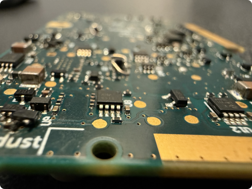
Test points are the primary interface between the DUT and the measurement system. To ensure easy access, a common best practice is to place all test points on a single side of the PCB. This simplifies the mechanical design of the test fixture by allowing probe contact from one side only, reducing fixture complexity.
It is not only important to position test points for mechanical accessibility but also to ensure that all critical electrical nodes required for testing are available. Careful selection of test points enables comprehensive test coverage across all components and signal paths on the PCB. This minimizes the risk of undetected faults and improves fault isolation during troubleshooting.
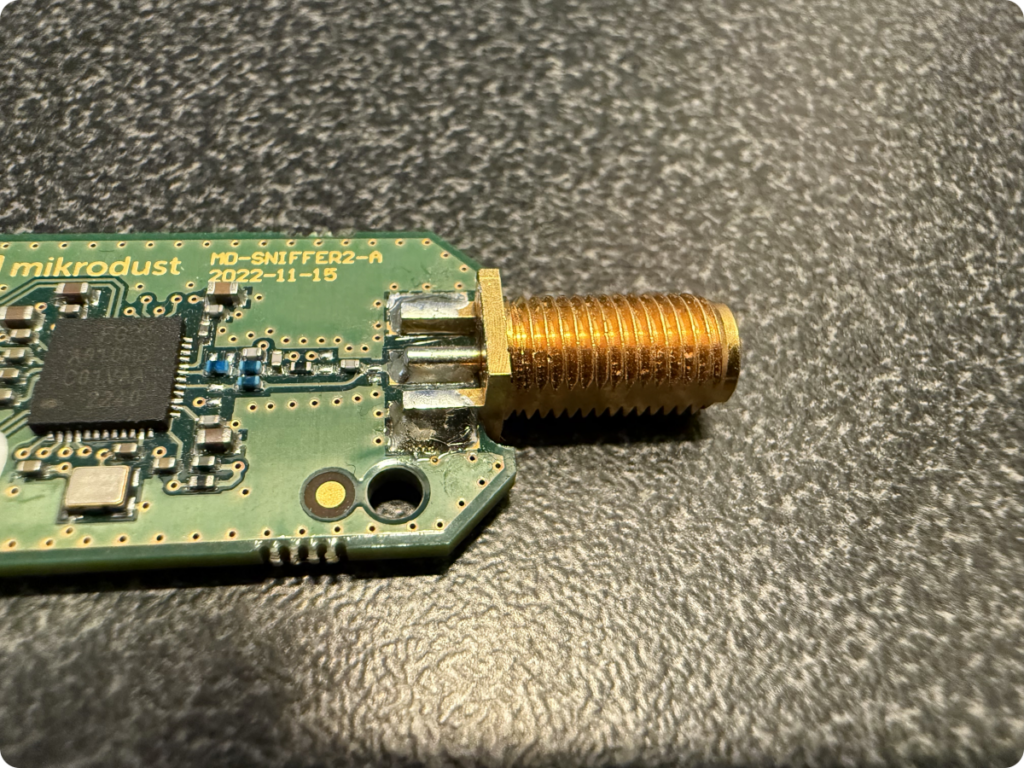
In designs where RF functionality is present and needs to be verified within a test fixture, it is recommended to include a dedicated RF test point. Radiated signal strength can vary significantly within the fixture due to interference and reflections. Providing an interface for conducted RF measurements improves test accuracy and repeatability by enabling direct signal measurement less affected by the fixture environment.
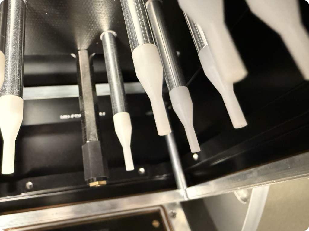
Pressure Support Pins
When using a bed-of-nails test fixture, it is important to allocate sufficient space not only for the test probes but also for mechanical support pins. These support pins distribute the force exerted by the test needles across the PCB, preventing flexing, bending, or damage during the test procedure.
This is especially critical for thin or mechanically sensitive PCBs. To mitigate this risk, it is good practice to provide space for support pins on the opposite side of the PCB in relation to the test needles.
Ready to optimize your testing? Contact us today for support and guidance